IMAGRAPH CORPORATION
ITX SERIES
|
Category |
Video |
|
Video Types Supported |
MGA/CGA/XVGA |
|
Video Processor |
Texas Instruments TMS34020 |
|
Highest Resolution Supported |
1280 x 1024 |
|
Data Bus Type |
16-bit ISA |
|
Memory Type |
DRAM/VRAM (factory installed) |
|
Maximum Onboard Memory |
2MB VRAM/16MB DRAM |

|
CONNECTIONS | |||
|
Purpose |
Location |
Purpose |
Location |
|
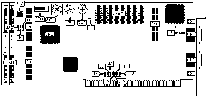
15-pin analog video port |
CN1 |
Diagnostic header |
J13 |
|
VGA pass-through |
CN2 |
Daughterboard headers |
P8-P10 |
|
SYNC ON GREEN CONFIGURATION | |
|
Mode |
SW4/1 |
|
Enabled |
On |
|
Disabled |
Off |
|
VIDEO EMULATION SELECTION | |||
|
» Mode |
SW4/5 |
SW4/6 | |
| » |
Disabled |
Off |
Off |
| » |
MDA |
On |
Off |
| » |
CGA |
Off |
On |
|
EMULATION EPROM CONFIGURATION | ||
|
» Setting |
J4 | |
| » |
Installed |
Pins 1 & 2 closed |
| » |
Not installed |
Pins 2 & 3 closed |
|
OUTPUT SYNC SIGNAL CONFIGURATION | ||
|
» Mode |
J1 | |
| » |
Composite sync |
Pins 1 & 2 closed |
| » |
Horizontal sync |
Pins 2 & 3 closed |
|
PASS-THROUGH SYNC SIGNAL CONFIGURATION | ||
|
» Mode |
J5 | |
| » |
Composite sync |
Pins 1 & 2 closed |
| » |
Horizontal sync |
Pins 2 & 3 closed |
|
INTERRUPT SELECTION | ||||||||
|
» IRQ |
J6 |
J7 |
J8 |
J9 |
J10 |
J11 |
J12 | |
| » |
Disabled |
Open |
Open |
Open |
Open |
Open |
Open |
Open |
| » |
2/9 |
Open |
Open |
Open |
Pins 2 & 3 |
Open |
Open |
Open |
| » |
3 |
Open |
Open |
Open |
Open |
Open |
Open |
Pins 2 & 3 |
| » |
4 |
Open |
Open |
Open |
Open |
Open |
Open |
Pins 1 & 2 |
| » |
5 |
Open |
Open |
Open |
Open |
Open |
Pins 2 & 3 |
Open |
| » |
6 |
Open |
Open |
Open |
Open |
Open |
Pins 1 & 2 |
Open |
| » |
7 |
Open |
Open |
Open |
Open |
Pins 2 & 3 |
Open |
Open |
| » |
10 |
Open |
Open |
Open |
Pins 1 & 2 |
Open |
Open |
Open |
| » |
11 |
Open |
Open |
Pins 2 & 3 |
Open |
Open |
Open |
Open |
| » |
12 |
Open |
Open |
Pins 1 & 2 |
Open |
Open |
Open |
Open |
| » |
14 |
Open |
Pins 2 & 3 |
Open |
Open |
Open |
Open |
Open |
| » |
15 |
Pins 1 & 2 |
Open |
Open |
Open |
Open |
Open |
Open |
|
Note: Pins designated are in the closed position. | ||||||||
|
BASE I/O ADDRESS SELECTION |
|
A total of 4096 memory address settings are available. The address is selected by setting the hexadecimal numerals on switches SW1-SW3. SW1 is the Most Significant Numeral, and SW3 is the Least Significant Numeral. For example, if SW1 = 2, SW2 = B, and SW3 = 0, the address would be 2B0h. |
|
DRAM CONFIGURATION | ||
|
Size |
Bank 0 |
Bank 1 |
|
1MB |
(1) 256K x 36 |
NONE |
|
2MB |
(1) 256K x 36 |
(1) 256K x 36 |
|
2MB |
(1) 512K x 36 |
NONE |
|
3MB |
(1) 512K x 36 |
(1) 256K x 36 |
|
4MB |
(1) 512K x 36 |
(1) 512K x 36 |
|
4MB |
(1) 1M x 36 |
NONE |
|
5MB |
(1) 1M x 36 |
(1) 256K x 36 |
|
6MB |
(1) 1M x 36 |
(1) 512K x 36 |
|
8MB |
(1) 1M x 36 |
(1) 1M x 36 |
|
8MB |
(1) 2M x 36 |
NONE |
|
9MB |
(1) 2M x 36 |
(1) 256K x 36 |
|
10MB |
(1) 2M x 36 |
(1) 512K x 36 |
|
12MB |
(1) 2M x 36 |
(1) 1M x 36 |
|
16MB |
(1) 2M x 36 |
(1) 2M x 36 |
|
FACTORY CONFIGURED - DO NOT ALTER | |
|
Jumper/Switch |
Position |
|
J2 |
Unidentified |
|
J3 |
Unidentified |
|
SW4/2 |
N/A |
|
SW4/3 |
N/A |
|
SW4/4 |
N/A |