UNIDENTIFIED
J-403TG 486 GREEN VLB (V2.0)
|
Processor |
80486SX/SL80486SX/80486DX/SL80486DX/CXM7/CXM72/80486DX4 |
|
Processor Speed |
25/33/40/50(internal)/66(internal)/100(internal)MHz |
|
Chip Set |
OPTI |
|
Video Chip Set |
None |
|
Maximum Onboard Memory |
128MB |
|
Maximum Video Memory |
None |
|
Cache |
64/128/256KB |
|
BIOS |
AMI/Award |
|
Dimensions |
254mm x 218mm |
|
I/O Options |
32-bit VESA local bus slots (3), green PC connector |
|
NPU Options |
None |
|
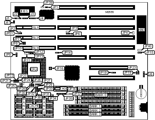
CONNECTIONS | |||
|
Purpose |
Location |
Purpose |
Location |
|
Turbo switch |
J1 |
External battery |
J6 |
|
Reset switch |
J2 |
Green PC connector |
JP16 |
|
Speaker |
J3 |
Green PC connector (monitor) |
JP19 |
|
Power LED & keylock |
J4 |
Green PC LED |
JP23 |
|
Turbo LED |
J5 |
32-bit VESA local bus slots |
SL1 - SL3 |
|
USER CONFIGURABLE SETTINGS | |||
|
Function |
Label |
Position | |
|
Jumper information unavailable |
JP2 |
Unidentified | |
|
Jumper information unavailable |
JP3 |
Unidentified | |
|
Jumper information unavailable |
JP4 |
Unidentified | |
|
Jumper information unavailable |
JP6 |
Unidentified | |
|
Jumper information unavailable |
JP11 |
Unidentified | |
|
Jumper information unavailable |
JP14 |
Unidentified | |
|
» |
CMOS memory normal operation |
JP15 |
Pins 2 & 3 closed |
|
CMOS memory clear |
JP15 |
Pins 1 & 2 closed | |
|
Jumper information unavailable |
JP29 |
Unidentified | |
|
Jumper information unavailable |
JP30 |
Unidentified | |
|
Jumper information unavailable |
JP37 |
Unidentified | |
|
Jumper information unavailable |
JP39 |
Unidentified | |
|
Jumper information unavailable |
JP40 |
Unidentified | |
|
Jumper information unavailable |
JP51 |
Unidentified | |
|
DRAM CONFIGURATION | ||||
|
Size |
Bank 0 |
Bank 1 |
Bank 2 |
Bank 3 |
|
2MB (A) |
(4) 256K x 9 |
(1) 256K x 36 |
None |
None |
|
2MB (B) |
None |
(1) 512K x 36 |
None |
None |
|
4MB (A) |
(4) 1M x 9 |
None |
None |
None |
|
4MB (B) |
None |
(1) 1M x 36 |
None |
None |
|
4MB (C) |
(4) 256K x 9 |
(1) 256K x 36 |
(1) 256K x 36 |
(1) 256K x 36 |
|
4MB (D) |
None |
(1) 512K x 36 |
(1) 512K x 36 |
None |
|
5MB |
(4) 256K x 9 |
(1) 1M x 36 |
None |
None |
|
6MB (A) |
(4) 256K x 9 |
(1) 256K x 36 |
(1) 1M x 36 |
None |
|
6MB (B) |
None |
(1) 512K x 36 |
(1) 1M x 36 |
None |
|
8MB (A) |
(4) 1M x 9 |
(1) 1M x 36 |
None |
None |
|
8MB (B) |
None |
(1) 2M x 36 |
None |
None |
|
8MB (C) |
None |
(1) 1M x 36 |
(1) 1M x 36 |
None |
|
10MB (A) |
(4) 256K x 9 |
(1) 256K x 36 |
(1) 2M x 36 |
None |
|
10MB (B) |
(4) 256K x 9 |
(1) 256K x 36 |
(1) 1M x 36 |
(1) 1M x 36 |
|
10MB (C) |
None |
(1) 512K x 36 |
(1) 2M x 36 |
None |
|
10MB (D) |
None |
(1) 512K x 36 |
(1) 1M x 36 |
(1) 1M x 36 |
|
12MB (A) |
(4) 1M x 9 |
None |
(1) 2M x 36 |
None |
|
12MB (B) |
None |
(1) 1M x 36 |
(1) 1M x 36 |
(1) 1M x 36 |
|
12MB (C) |
(4) 1M x 9 |
None |
(1) 1M x 36 |
(1) 1M x 36 |
|
16MB (A) |
(4) 4M x 9 |
None |
None |
None |
|
16MB (B) |
None |
(1) 4M x 36 |
None |
None |
|
16MB (C) |
(4) 1M x 9 |
(1) 1M x 36 |
(1) 1M x 36 |
(1) 1M x 36 |
|
16MB (D) |
None |
(1) 2M x 36 |
(1) 2M x 36 |
None |
|
17MB |
(4) 256K x 9 |
(1) 4M x 36 |
None |
None |
|
20MB (A) |
(4) 1M x 9 |
(1) 4M x 36 |
None |
None |
|
DRAM CONFIGURATION (CON’T) | ||||
|
Size |
Bank 0 |
Bank 1 |
Bank 2 |
Bank 3 |
|
20MB (B) |
(4) 1M x 9 |
None |
(1) 4M x 36 |
None |
|
20MB (C) |
None |
(1) 1M x 36 |
(1) 4M x 36 |
None |
|
32MB (A) |
(4) 4M x 9 |
(1) 4M x 36 |
None |
None |
|
32MB (B) |
None |
(1) 8M x 36 |
None |
None |
|
32MB (C) |
(4) 4M x 9 |
None |
(1) 4M x 36 |
None |
|
32MB (D) |
None |
(1) 4M x 36 |
(1) 4M x 36 |
None |
|
64MB (A) |
(4) 16M x 9 |
None |
None |
None |
|
64MB (B) |
None |
(1) 16M x 36 |
None |
None |
|
64MB (C) |
(4) 4M x 9 |
(1) 4M x 36 |
(1) 4M x 36 |
(1) 4M x 36 |
|
64MB (D) |
None |
(1) 8M x 36 |
(1) 8M x 36 |
None |
|
128MB (A) |
(4) 16M x 9 |
(1) 16M x 36 |
None |
None |
|
128MB (B) |
None |
(1) 32M x 36 |
None |
None |
|
128MB (C) |
(4) 16M x 9 |
None |
(1) 16M x 36 |
None |
|
128MB (D) |
None |
(1) 16M x 36 |
(1) 16M x 36 |
None |
|
DRAM JUMPER CONFIGURATION | |
|
Size |
JP18 |
|
2MB (A) |
Pins 1 & 2 closed |
|
2MB (B) |
Pins 2 & 3 closed |
|
4MB (A) |
Pins 1 & 2 closed |
|
4MB (B) |
Pins 2 & 3 closed |
|
4MB (C) |
Pins 1 & 2 closed |
|
4MB (D) |
Pins 2 & 3 closed |
|
5MB |
Pins 1 & 2 closed |
|
6MB (A) |
Pins 1 & 2 closed |
|
6MB (B) |
Pins 2 & 3 closed |
|
8MB (A) |
Pins 1 & 2 closed |
|
8MB (B) |
Pins 2 & 3 closed |
|
8MB (C) |
Pins 2 & 3 closed |
|
10MB (A) |
Pins 1 & 2 closed |
|
10MB (B) |
Pins 1 & 2 closed |
|
10MB (C) |
Pins 2 & 3 closed |
|
10MB (D) |
Pins 2 & 3 closed |
|
12MB (A) |
Pins 1 & 2 closed |
|
12MB (B) |
Pins 2 & 3 closed |
|
12MB (C) |
Pins 1 & 2 closed |
|
16MB (A) |
Pins 1 & 2 closed |
|
16MB (B) |
Pins 2 & 3 closed |
|
16MB (C) |
Pins 1 & 2 closed |
|
16MB (D) |
Pins 2 & 3 closed |
|
17MB |
Pins 1 & 2 closed |
|
20MB (A) |
Pins 1 & 2 closed |
|
DRAM JUMPER CONFIGURATION (CON’T) | |
|
Size |
JP18 |
|
20MB (B) |
Pins 1 & 2 closed |
|
20MB (C) |
Pins 2 & 3 closed |
|
32MB (A) |
Pins 1 & 2 closed |
|
32MB (B) |
Pins 2 & 3 closed |
|
32MB (C) |
Pins 1 & 2 closed |
|
32MB (D) |
Pins 2 & 3 closed |
|
64MB (A) |
Pins 1 & 2 closed |
|
64MB (B) |
Pins 2 & 3 closed |
|
64MB (C) |
Pins 1 & 2 closed |
|
64MB (D) |
Pins 2 & 3 closed |
|
128MB (A) |
Pins 1 & 2 closed |
|
128MB (B) |
Pins 2 & 3 closed |
|
128MB (C) |
Pins 1 & 2 closed |
|
128MB (D) |
Pins 2 & 3 closed |
|
CACHE CONFIGURATION | |||
|
Size |
Bank 0 |
Bank 1 |
TAG |
|
64KB |
(4) 8K x 8 |
(4) 8K x 8 |
(1) 8K x 8 |
|
128KB |
(4) 32K x 8 |
None |
(1) 8K x 8 |
|
256KB (A) |
(4) 32K x 8 |
(4) 32K x 8 |
(1) 32K x 8 |
|
256KB (B) |
(4) 32K x 8 |
(4) 32K x 8 |
(1) 16K x 8 |
|
CACHE JUMPER CONFIGURATION | ||||
|
Size |
JP34 |
JP35 |
JP36 |
JP38 |
|
64KB |
Pins 1 & 2 closed |
Open |
Open |
Pins 2 & 3 closed |
|
128KB |
Pins 1 & 2 closed |
Closed |
Open |
Pins 1 & 2 closed |
|
256KB (A) |
Pins 1 & 2 closed |
Closed |
Closed |
Pins 2 & 3 closed |
|
256KB (B) |
Pins 2 & 3 closed |
Closed |
Closed |
Pins 2 & 3 closed |
|
CPU SPEED SELECTION (AV-9107-03) | |||||
|
Speed |
JP9 |
JP21 |
JP22 |
JP23 |
JP24 |
|
25MHz |
1 & 2 |
Open |
Closed |
Open |
Closed |
|
33MHz |
1 & 2 |
Open |
Closed |
Closed |
Open |
|
40MHz |
1 & 2 |
Open |
Open |
Open |
Closed |
|
50iMHz |
1 & 2 |
Open |
Closed |
Open |
Closed |
|
66iMHz |
1 & 2 |
Open |
Closed |
Closed |
Open |
|
100iMHz |
1 & 2 |
Open |
Closed |
Closed |
Open |
|
Note: Pins designated should be in the closed position. | |||||
|
CPU SPEED SELECTION (SC468) | |||||
|
Speed |
JP9 |
JP21 |
JP22 |
JP23 |
JP24 |
|
25MHz |
Open |
Open |
Open |
Open |
Open |
|
33MHz |
Open |
Open |
Closed |
Closed |
Open |
|
40MHz |
Open |
Open |
Open |
Closed |
Open |
|
50iMHz |
Open |
Open |
Open |
Open |
Open |
|
66iMHz |
Open |
Open |
Closed |
Closed |
Open |
|
100iMHz |
Open |
Open |
Closed |
Closed |
Open |
|
CPU TYPE SELECTION | |||||
|
Type |
JP1 |
JP10 |
JP12 |
JP13 |
JP26 |
|
80486SX |
Open |
Open |
Open |
Open |
Open |
|
SL80486SX |
Closed |
Open |
Open |
Open |
Open |
|
80486DX |
Open |
Open |
Open |
Open |
1 & 2 |
|
SL80486DX |
Closed |
Open |
Open |
Open |
1 & 2 |
|
CX M7 |
Open |
1 & 2 |
Open |
2 & 3 |
1 & 2 |
|
CX M72 |
Open |
1 & 2 |
Open |
2 & 3 |
1 & 2 |
|
80486DX2 |
Open |
Open |
Open |
Open |
1 & 2 |
|
SL80486DX2 |
Closed |
Open |
Open |
Open |
1 & 2 |
|
80486DX4 |
Closed |
Open |
Open |
1 & 2 |
1 & 2 |
|
Note: Pins designated should be in the closed position. | |||||
|
CPU TYPE SELECTION (CON’T) | |||||
|
Type |
JP27 |
JP28 |
JP31 |
JP32 |
JP33 |
|
80486SX |
2 & 3 |
1 & 2 |
Open |
Open |
Open |
|
SL80486SX |
2 & 3 |
1 & 2 |
1 & 2 |
Closed |
Closed |
|
80486DX |
1 & 2, 3 & 4 |
1 & 2 |
Open |
Open |
Open |
|
SL80486DX |
1 & 2, 3 & 4 |
1 & 2 |
1 & 2 |
Closed |
Closed |
|
CX M7 |
1 & 2, 3 & 4 |
2 & 3 |
2 & 3 |
Open |
Open |
|
CX M72 |
1 & 2, 3 & 4 |
2 & 3 |
2 & 3 |
Open |
Open |
|
80486DX2 |
1 & 2, 3 & 4 |
1 & 2 |
Open |
Open |
Open |
|
SL80486DX2 |
1 & 2, 3 & 4 |
1 & 2 |
1 & 2 |
Closed |
Closed |
|
80486DX4 |
1 & 2, 3 & 4 |
1 & 2 |
1 & 2 |
Closed |
Closed |
|
Note: Pins designated should be in the closed position. | |||||
|
CPU VOLTAGE SELECTION | |
|
Voltage |
JP25 |
|
3.3v |
Pins 3 & 5, 4 & 6 closed |
|
5v |
Pins 1 & 3, 2 & 4 closed |
|
VL BUS SPEED SELECTION | |
|
Speed |
JP7 |
|
< = 33MHz |
Open |
|
> 33MHz |
Closed |
|
VL BUS WAIT STATE SELECTION | |
|
Setting |
JP8 |
|
0 |
Open |
|
1 |
Closed |