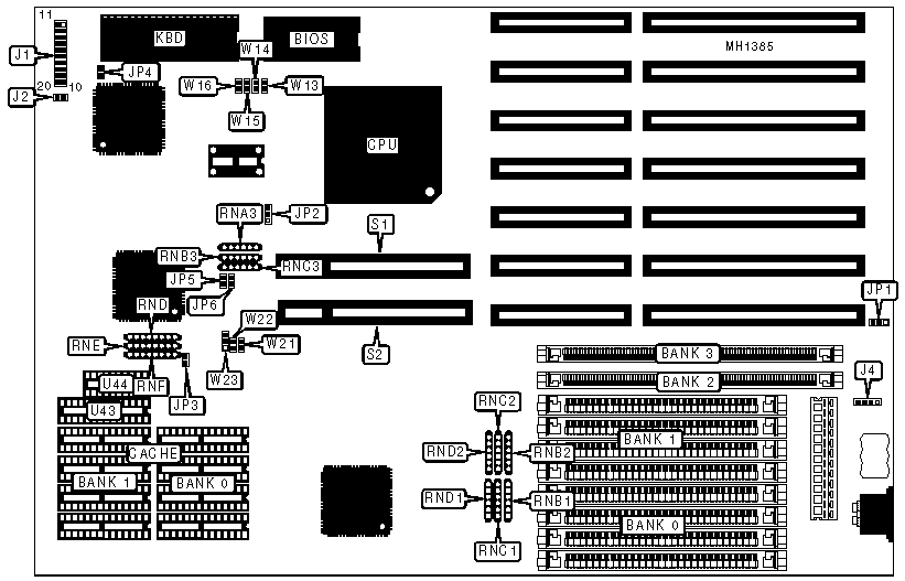
TMC RESEARCH CORPORATION
PAT48PR
|
Processor |
80486SX/80487SX/80486DX/ODP486SX/80486DX2 |
|
Processor Speed |
25/33/50(internal)/50/66(internal)MHz |
|
Chip Set |
OPTI |
|
Max. Onboard DRAM |
64MB |
|
SRAM Cache |
64/128/256KB |
|
BIOS |
AMI |
|
Dimensions |
220mm x 240mm |
|
I/O Options |
32-bit VESA local bus slot (2) |
|
NPU Options |
None |
|
|
|
|
CONNECTIONS |
|||
|
Purpose |
Location |
Purpose |
Location |
|
Speaker |
J1/pins 1-4 |
IDE interface LED |
J1 pins 10 & 20 |
|
Turbo switch |
J1/pins 7 & 17 |
IDE interface LED |
J2 |
|
Turbo LED |
J1/pins 8 & 18 |
External battery |
J4 |
|
Reset switch |
J1/pins 9 & 19 |
32-bit VESA local bus card (2) |
S1 & S2 |
|
USER CONFIGURABLE SETTINGS |
|||
|
Function |
Jumper |
Position |
|
|
» |
CMOS memory normal operation (internal battery) |
JP1 |
pins 2 & 3 closed |
|
» |
CMOS memory normal operation (external battery) |
JP1 |
open |
|
|
CMOS memory clear |
JP1 |
pins 1 & 2 closed |
|
» |
Monitor type select color |
JP4 |
closed |
|
|
Monitor type select monochrome |
JP4 |
open |
|
DRAM CONFIGURATION |
||||||
|
Size |
Bank 0 |
Bank 1 |
Bank 2 |
Bank 3 |
RNB1 & RNB2 |
RNC1 & RNC2 |
|
1MB |
(4) 256K x 9 |
NONE |
NONE |
NONE |
open |
closed |
|
2MB |
(4) 256K x 9 |
(4) 256K x 9 |
NONE |
NONE |
open |
closed |
|
4MB |
(4) 1M x 9 |
NONE |
NONE |
NONE |
open |
closed |
|
4MB |
NONE |
NONE |
(1) 1M x 36 |
NONE |
closed |
open |
|
5MB |
(4) 1M x 9 |
(4) 256K x 9 |
NONE |
NONE |
open |
closed |
|
6MB |
(4) 256K x 9 |
(4) 256K x 9 |
(1) 1M x 36 |
NONE |
open |
closed |
|
8MB |
(4) 1M x 9 |
(4) 1M x 9 |
NONE |
NONE |
open |
closed |
|
8MB |
NONE |
NONE |
(1) 1M x 36 |
(1) 1M x 36 |
closed |
open |
|
9MB |
(4) 256K x 9 |
(4) 1M x 9 |
(1) 1M x 36 |
NONE |
open |
closed |
|
10MB |
(4) 256K x 9 |
(4) 256K x 9 |
(1) 1M x 36 |
(1) 1M x 36 |
open |
closed |
|
12MB |
(4) 1M x 9 |
(4) 1M x 9 |
(1) 1M x 36 |
NONE |
open |
closed |
|
13MB |
(4) 256K x 9 |
(4) 1M x 9 |
(1) 1M x 36 |
(1) 1M x 36 |
open |
closed |
|
16MB |
(4) 1M x 9 |
(4) 1M x 9 |
(1) 1M x 36 |
(1) 1M x 36 |
open |
closed |
|
16MB |
(4) 4M x 9 |
NONE |
NONE |
NONE |
open |
closed |
|
16MB |
NONE |
NONE |
(1) 4M x 36 |
NONE |
closed |
open |
|
20MB |
(4) 4M x 9 |
(4) 1M x 9 |
NONE |
NONE |
open |
closed |
|
20MB |
NONE |
NONE |
(1) 4M x 36 |
(1) 1M x 36 |
closed |
open |
|
24MB |
(4) 4M x 9 |
(4) 1M x 9 |
(1) 1M x 36 |
NONE |
open |
closed |
|
28MB |
(4) 4M x 9 |
(4) 1M x 9 |
(1) 1M x 36 |
(1) 1M x 36 |
open |
closed |
|
32MB |
(4) 4M x 9 |
(4) 4M x 9 |
NONE |
NONE |
open |
closed |
|
32MB |
NONE |
NONE |
(1) 4M x 36 |
(1) 4M x 36 |
closed |
open |
|
36MB |
(4) 4M x 9 |
(4) 4M x 9 |
(1) 1M x 36 |
NONE |
open |
closed |
|
40MB |
(4) 4M x 9 |
(4) 4M x 9 |
(1) 1M x 36 |
(1) 1M x 36 |
open |
closed |
|
48MB |
(4) 4M x 9 |
(4) 4M x 9 |
(1) 4M x 36 |
NONE |
open |
closed |
|
52MB |
(4) 4M x 9 |
(4) 4M x 9 |
(1) 4M x 36 |
(1) 1M x 36 |
open |
closed |
|
52MB |
(4) 4M x 9 |
(4) 1M x 9 |
(1) 4M x 36 |
(1) 4M x 36 |
open |
closed |
|
64MB |
(4) 4M x 9 |
(4) 4M x 9 |
(1) 4M x 36 |
(1) 4M x 36 |
open |
closed |
|
SRAM CONFIGURATION |
||||
|
Size |
Cache |
Location |
TAG(U43) |
TAG(U44) |
|
64KB |
(8) 8K x 8 |
Banks 0 & 1 |
(1) 8K x 8 |
(1) 64K x 1 |
|
128KB |
(4) 32K x 8 |
Bank 0 |
(1) 8K x 8 |
(1) 64K x 1 |
|
256KB |
(8) 32K x 8 |
Banks 0 & 1 |
(1) 32K x 8 |
(1) 64K x 1 |
|
SRAM RESISTOR CONFIGURATION |
|||
|
Size |
RND |
RNE |
RNF |
|
64KB |
closed |
open |
open |
|
128KB |
open |
closed |
open |
|
256KB |
open |
open |
closed |
|
CPU JUMPER CONFIGURATION |
|||
|
CPU |
RNA3 |
RNB3 |
RNC3 |
|
80486DX2 |
closed |
open |
open |
|
ODP486SX |
open |
closed |
open |
|
80486DX |
closed |
open |
open |
|
80487SX |
open |
closed |
open |
|
80486SX |
open |
open |
closed |
|
VESA CARDS SUPPORTED JUMPER CONFIGURATION |
|||
|
# of VESA cards |
W21 |
W22 |
W23 |
|
2 |
closed |
closed |
pins 1 & 2 closed |
|
1 |
W21/pin 1 connected to W22/pin1 |
pins 2 & 3 closed |
|
|
Note: The manufacturer recommends that only one VESA card be used with a 486DX-50MHz. |
|||
|
CPU SPEED JUMPER CONFIGURATION |
|||||||
|
CPU |
JP2 |
JP3 |
JP5 & JP6 |
W13 |
W14 |
W15 |
W16 |
|
25MHz |
pins 2 & 3 |
pins 1 & 2 |
open |
open |
open |
closed |
open |
|
33MHz |
pins 2 & 3 |
pins 1 & 2 |
open |
open |
open |
open |
closed |
|
50iMHz |
pins 2 & 3 |
pins 1 & 2 |
open |
open |
open |
closed |
open |
|
50MHz |
pins 1 & 2 |
pins 2 & 3 |
closed |
open |
open |
closed |
open |
|
66iMHz |
pins 2 & 3 |
pins 1 & 2 |
open |
open |
open |
open |
closed |
|
Note:W13 - W16 need only be configured if a 20-pin clock generator is installed in U29. JP3 is AT bus clock select. JP5 and JP6 are VESA bus clock select. Pins designated are in the closed position. |
|||||||