TMC RESEARCH CORPORATION
PET48PX
|
Processor |
80486SX//80487SX/80486DX/ODP486SX/80486DX2 |
|
Processor Speed |
20/25/33/50(internal)/50/66(internal)MHz |
|
Chip Set |
OPTI |
|
Max. Onboard DRAM |
128MB |
|
SRAM Cache |
64/128/256KB |
|
BIOS |
AMI |
|
Dimensions |
330.2mm x 218.4mm |
|
I/O Options |
None |
|
NPU Options |
4167 |

|
CONNECTIONS |
|||
|
Purpose |
Location |
Purpose |
Location |
|
IDE interface LED (input) |
J4 |
Reset switch |
J5/pins 9 & 19 |
|
Speaker |
J5/pins 1-4 |
IDE interface LED (output) |
J5/pins 10 & 20 |
|
Turbo switch |
J5/pins 7 & 17 |
Power LED & keylock |
J5/pins 11 - 15 |
|
Turbo LED |
J5/pins 8 & 18 |
|
|
|
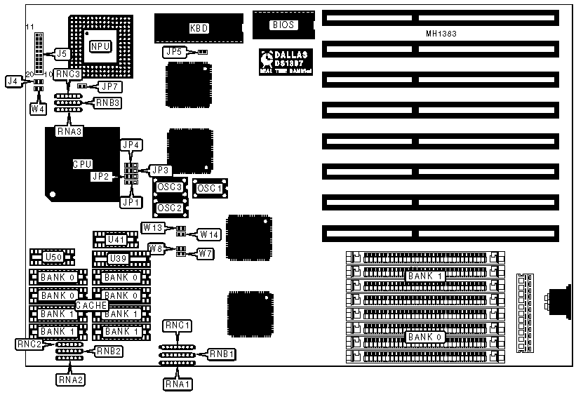
Note: Connect the chassis HD LED to J1/pins 10 & 20 then connect the hard drive LED jumper on the drive controller to J4. |
|||
|
USER CONFIGURABLE SETTINGS |
|||
|
Function |
Jumper |
Position |
|
|
» |
Monitor type select color |
JP5 |
closed |
|
|
Monitor type select monochrome |
JP5 |
open |
|
» |
EISA mode select CHRDY |
JP7 |
open |
|
|
EISA mode select EXRDY |
JP7 |
closed |
|
Note: Some older EISA cards use EXRDY (JP7 closed) to signal the completion of an ISA slave cycle. |
|||
|
DRAM CONFIGURATION |
||
|
Size |
Bank 0 |
Bank 1 |
|
4MB |
(4) 1M x 9 |
NONE |
|
8MB |
(4) 1M x 9 |
(4) 1M x 9 |
|
16MB |
(4) 4M x 9 |
NONE |
|
20MB |
(4) 1M x 9 |
(4) 4M x 9 |
|
32MB |
(4) 4M x 9 |
(4) 4M x 9 |
|
64MB |
(4) 16M x 9 |
NONE |
|
128MB |
(4) 16M x 9 |
(4) 16M x 9 |
|
SRAM CONFIGURATION |
||||||
|
Size |
Max. Cacheable |
Cache |
Location |
TAG (U39) |
TAG (U41) |
TAG (U50) |
|
64KB |
32MB |
(8) 8K x 8 |
Banks 0 & 1 |
(1) 8K x 8 |
(1) 16K x 1 |
(1) 16K x 1 |
|
128KB |
64MB |
(4) 32K x 8 |
Bank 0 |
(1) 8K x 8 |
(1) 16K x 1 |
(1) 16K x 1 |
|
256KB |
128MB |
(8) 32K x 8 |
Banks 0 & 1 |
(1) 32K x 8 |
(1) 16K x 1 |
(1) 16K x 1 |
|
Note:U41 & U50 will accept 64K x 1 or 16k x 1 chips in all configurations. When installing chips in sockets U41 & U50 the chips should be inserted into the socket from the side opposite pin 1. (Pin 1 of the chip still faces pin 1 of the socket.) With a 16K x 1 chip this will leave 2 empty holes on the side of pin1. This is normal. (see diagram below)
|
||||||
|
SRAM JUMPER CONFIGURATION |
|||
|
Resistor |
64KB |
128KB |
256KB |
|
RNA1 |
closed |
open |
open |
|
RNB1 |
open |
closed |
open |
|
RNC1 |
open |
open |
closed |
|
RNA2 |
closed |
open |
open |
|
RNB2 |
open |
closed |
open |
|
RNC2 |
open |
open |
closed |
|
CPU RESISTOR NETWORK CONFIGURATION |
|||
|
CPU |
RNA3 |
RNB3 |
RNC3 |
|
80486SX |
open |
open |
closed |
|
80487SX |
open |
closed |
open |
|
80486DX |
closed |
open |
open |
|
ODP486SX |
open |
closed |
open |
|
80486DX2 |
closed |
open |
open |
|
CPU SPEED CONFIGURATION |
||||||||||
|
CPU |
iOSC |
JP1 |
JP2 |
JP3 |
JP4 |
W4 |
W7 |
W8 |
W13 |
W14 |
|
20MHz |
40MHz |
2 & 3 |
1 & 2 |
1 & 2 |
2 & 3 |
closed |
closed |
open |
open |
open |
|
25MHz |
50MHz |
1 & 2 |
1 & 2 |
1 & 2 |
2 & 3 |
open |
open |
open |
open |
open |
|
33MHz |
66MHz |
1 & 2 |
1 & 2 |
2 & 3 |
2 & 3 |
open |
open |
closed |
open |
open |
|
50iMHz |
50MHz |
1 & 2 |
1 & 2 |
1 & 2 |
2 & 3 |
open |
open |
open |
open |
open |
|
50MHz |
50MHz |
1 & 2 |
2 & 3 |
2 & 3 |
1 & 2 |
open |
open |
open |
open |
open |
|
66iMHz |
66MHz |
1 & 2 |
1 & 2 |
2 & 3 |
2 & 3 |
open |
open |
closed |
open |
open |
|
Note: Pins designated should be in the closed position. |
||||||||||