FIRST INTERNATIONAL COMPUTER, INC.
486-JAL REV. C
|
Processor |
80486SX/80486DX/80486DX2 |
|
Processor Speed |
25/33/50(internal)/66(internal)MHz |
|
Chip Set |
VIA |
|
Max. Onboard DRAM |
32MB |
|
Cache |
64/128/256KB |
|
BIOS |
AMI |
|
Dimensions |
330mm x 218mm |
|
I/O Options |
PS/2 mouse port, parallel port, serial ports (2), VGA port, VGA feature connector, floppy drive interface, IDE interface, riser card |
|
NPU Options |
None |
|
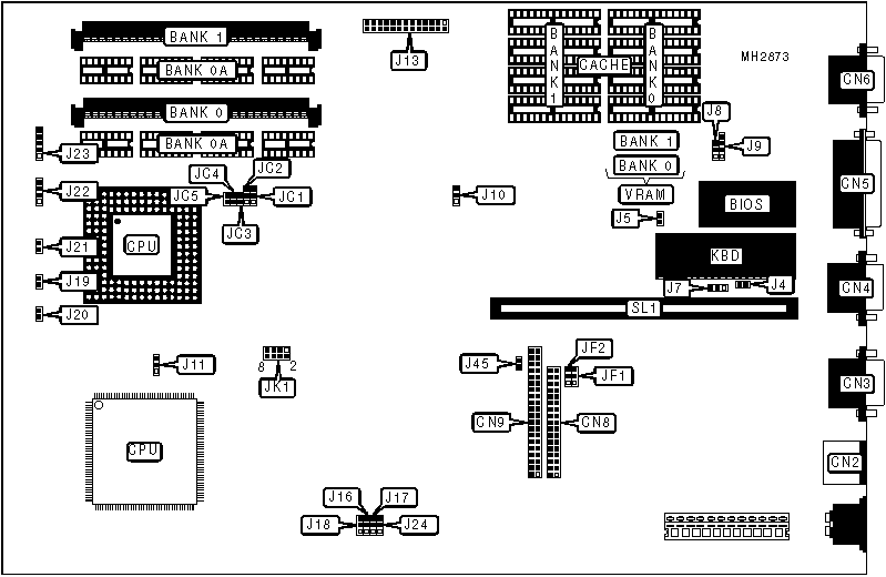
CONNECTIONS | |||
|
Purpose |
Location |
Purpose |
Location |
|
PS/2 mouse port |
CN2 |
VGA feature connector |
J13 |
|
Serial port 1 |
CN3 |
Turbo switch |
J19 |
|
Serial port 2 |
CN4 |
Turbo LED |
J20 |
|
Parallel port |
CN5 |
Reset switch |
J21 |
|
VGA port |
CN6 |
Speaker |
J22 |
|
Floppy drive interface |
CN8 |
Power LED & keylock |
J23 |
|
IDE interface |
CN9 |
IDE interface LED |
J45 |
|
External battery |
J9 |
Riser Card |
SL1 |
|
USER CONFIGURABLE SETTINGS | |||
|
Function |
Jumper |
Position | |
|
» |
Monitor type select monochrome/EGA/VGA |
J4 |
Open |
|
Monitor type select color |
J4 |
Closed | |
|
» |
CMOS memory normal operation |
J5 |
Open |
|
CMOS memory clear |
J5 |
Closed | |
|
» |
Password normal operation |
J7 |
Open |
|
Password reset |
J7 |
pins 2 & 3 closed | |
|
» |
Battery type select internal |
J8 |
pins 2 & 3 closed |
|
Battery type select external |
J8 |
pins 1 & 2 closed | |
|
» |
On board VGA enabled |
J10 |
pins 1 & 2 closed |
|
On board VGA disabled |
J10 |
pins 2 & 3 closed | |
|
» |
Factory configured - do not alter |
J11 |
N/A |
|
» |
IDE interface enabled |
J24 |
pins 1 & 2 closed |
|
IDE interface disabled |
J24 |
pins 2 & 3 closed | |
|
» |
Factory configured - do not alter |
JC5 |
N/A |
|
DRAM CONFIGURATION 1 | ||
|
Size |
Bank 0 |
Bank 1 |
|
1MB |
(1) 256K x 36 |
NONE |
|
2MB |
(1) 256K x 36 |
(1) 256K x 36 |
|
4MB |
(1) 1M x 36 |
NONE |
|
5MB |
(1) 1M x 36 |
(1) 256K x 36 |
|
8MB |
(1) 1M x 36 |
(1) 1M x 36 |
|
16MB |
(1) 4M x 36 |
NONE |
|
17MB |
(1) 4M x 36 |
(1) 256K x 36 |
|
20MB |
(1) 4M x 36 |
(1) 1M x 36 |
|
32MB |
(1) 4M x 36 |
(1) 4M x 36 |
|
DRAM CONFIGURATION 2 | ||
|
Size |
Bank 0A |
Bank 1 |
|
4MB |
4MB |
NONE |
|
5MB |
4MB |
(1) 256K x 36 |
|
8MB |
4MB |
(1) 1M x 36 |
|
20MB |
4MB |
(1) 4M x 36 |
|
Note: Bank 0A is factory installed and is not configurable. Use either this table or the above table. | ||
|
CACHE CONFIGURATION | ||
|
Size |
Bank 0 |
Bank 1 |
|
64KB |
(4) 8K x 8 |
(4) 8K x 8 |
|
128KB |
(4) 32K x 8 |
NONE |
|
256KB |
(4) 32K x 8 |
(4) 32K x 8 |
|
CPU TYPE CONFIGURATION | ||||
|
Type |
JC1 |
JC2 |
JC3 |
JC4 |
|
80486SX |
pins 2 & 3 closed |
pins 2 & 3 closed |
Open |
Open |
|
80486DX |
pins 1 & 2 closed |
pins 1 & 2 closed |
Closed |
Closed |
|
80486DX2 |
pins 1 & 2 closed |
pins 1 & 2 closed |
Closed |
Closed |
|
CPU SPEED CONFIGURATION | |
|
Speed |
JK1 |
|
25MHz |
pins 5 & 6 closed |
|
33MHz |
pins 1 & 2 closed |
|
50iMHz |
pins 5 & 6 closed |
|
66iMHz |
pins 1 & 2 closed |
|
HARD DRIVE SPEED CONFIGURATION | ||
|
Speed |
J16 |
J17 |
|
0 |
pins 2 & 3 closed |
pins 2 & 3 closed |
|
1 |
pins 1 & 2 closed |
pins 2 & 3 closed |
|
2 |
pins 1 & 2 closed |
pins 1 & 2 closed |
|
BUS SPEED CONFIGURATION | |
|
CPU speed |
J18 |
|
<= 33MHz |
pins 1 & 2 closed |
|
> 33MHz |
pins 2 & 3 closed |
|
FLOPPY DRIVE CONFIGURATION | ||
|
Type |
JF1 |
JF2 |
|
1.44MB |
pins 2 & 3 closed |
pins 2 & 3 closed |
|
2.88MB |
pins 1 & 2 closed |
pins 1 & 2 closed |
|
VRAM CONFIGURATION | ||
|
Size |
Bank 0 |
Bank 1 |
|
512KB |
512KB |
NONE |
|
1MB |
512KB |
512KB |
|
2MB |
1MB |
1MB |
|
Note: The size of the VRAM chips are unidentified. | ||