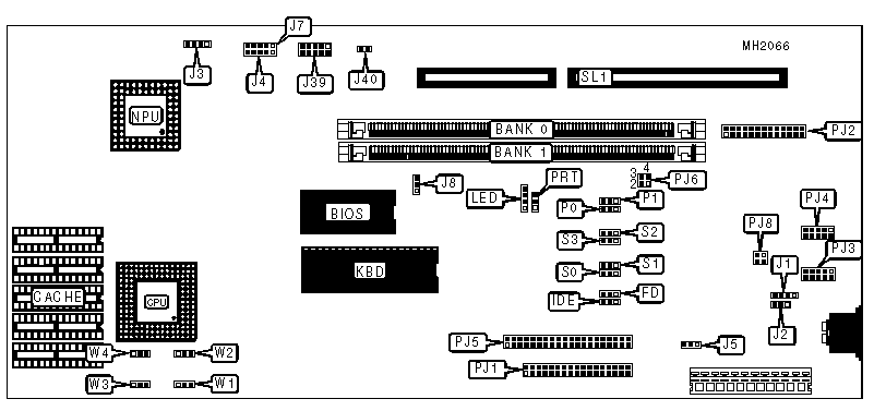
CSS LABORATORIES, INC.
MINIMAX 333
|
Processor |
80386DX |
|
Processor Speed |
8/33MHz |
|
Chip Set |
C & T |
|
Max. Onboard DRAM |
16MB |
|
Cache |
32/64/128KB |
|
BIOS |
AMI |
|
I/O Options |
16-bit external memory card slot, floppy drive interface, IDE interface, parallel port, serial ports (2) |
|
NPU Options |
80387DX |

|
CONNECTIONS | |||
|
Purpose |
Location |
Purpose |
Location |
|
External battery |
J1 |
Floppy drive interface |
PJ1 |
|
Reset switch |
J2 |
Parallel port |
PJ2 |
|
Power LED & keylock |
J3 |
Serial port 1 |
PJ3 |
|
Speaker |
J7 |
Serial port 2 |
PJ4 |
|
Equipment panel connector |
J39 |
IDE interface connector |
PJ5 |
|
Hard drive access LED connector |
J40 |
16-bit external memory card slot |
SL1 |
|
IDE access light connector |
LED | ||
|
USER CONFIGURABLE SETTINGS | |||
|
Function |
Jumper |
Position | |
|
» |
On-board floppy drive controller enabled |
FD |
pins 2 & 3 closed |
|
On-board floppy drive controller disabled |
FD |
pins 1 & 2 closed | |
|
» |
On-board IDE disk controller enabled |
IDE |
pins 2 & 3 closed |
|
On-board IDE disk controller disabled |
IDE |
pins 1 & 2 closed | |
|
» |
Factory configured - do not alter |
J4 |
N/A |
|
» |
Color or EGA adaptor enabled |
J5 |
pins 2 & 3 closed |
|
Monochrome adaptor enabled |
J5 |
pins 1 & 2 closed | |
|
Type 1 memory selector single sided SIMM |
J8 |
pins 1 & 2 closed | |
|
Type 2 memory selector double sided SIMM |
J8 |
pins 2 & 3 closed | |
|
» |
Factory configured - do not alter |
PJ8 |
N/A |
|
SERIAL PORT 1 CONFIGURATION | |||||
|
COM |
IRQ |
I/O Address |
PJ6 |
S0 |
S1 |
|
N/A |
N/A |
Disable |
N/A |
pins 1 & 2 |
pins 1 & 2 |
|
COM2 |
IRQ3 |
2F8h |
pins 1 & 3 |
pins 1 & 2 |
pins 2 & 3 |
|
COM1 |
IRQ4 |
3F8h |
pins 1 & 2 |
pins 2 & 3 |
pins 2 & 3 |
|
Note:Pins designated are in the closed position. | |||||
|
SERIAL PORT 2 CONFIGURATION | |||||
|
COM |
IRQ |
I/O Address |
PJ6 |
S2 |
S3 |
|
N/A |
N/A |
Disable |
N/A |
pins 1 & 2 |
pins 1 & 2 |
|
COM1 |
IRQ4 |
3F8h |
pins 2 & 4 |
pins 1 & 2 |
pins 2 & 3 |
|
COM2 |
IRQ3 |
2F8h |
pins 3 & 4 |
pins 2 & 3 |
pins 2 & 3 |
|
Note:Pins designated are in the closed position. | |||||
|
PARALLEL PORT CONFIGURATION | |||||
|
LPT |
IRQ |
I/0 Address |
P0 |
P1 |
PRT |
|
N/A |
N/A |
Disable |
pins 1 & 2 |
pins 1 & 2 |
N/A |
|
LPT3 |
IRQ7 |
378h |
pins 1 & 2 |
pins 2 & 3 |
pins 2 & 3 |
|
LPT2 |
IRQ5 |
278h |
pins 2 & 3 |
pins 2 & 3 |
pins 1 & 2 |
|
LPT1 |
IRQ7 |
3BCh |
pins 2 & 3 |
pins 1 & 2 |
pins 2 & 3 |
|
Note:Pins designated are in the closed position. | |||||
|
DRAM CONFIGURATION | ||
|
Size |
Bank 0 |
Bank 1 |
|
1MB |
(1) 256K x 36 |
NONE |
|
2MB |
(1) 256K x 36 |
(1) 256K x 36 |
|
4MB |
(1) 512K x 36 |
(1) 512K x 36 |
|
5MB |
(1) 1M x 36 |
(1) 256K x 36 |
|
8MB |
(1) 1M x 36 |
(1) 1M x 36 |
|
10MB |
(1) 512K x 36 |
(1) 2M x 36 |
|
16MB |
(1) 2M x 36 |
(1) 2M x 36 |
|
MISCELLANEOUS TECHNICAL NOTES |
|
Note:The cache on the MINIMAX 333 is soldered on the board and is non configurable. The cache comes in 32K, 64K, and 128K. Jumpers W1 -W4 are for cache configuration that is not available on this board, but is available on other boards made by this manufacturer. ( a 486 version of the MINIMAX 333) |