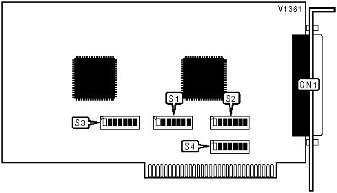
SYNERGY SOLUTIONS
SS-558
|
Card Type |
Serial card |
|
Chipset Controller |
16C554 UART (2) |
|
I/O Options |
Serial port (8 serial port connectors on external cable) |
|
Maximum DRAM |
N/A |

|
CONNECTIONS | |
|
Purpose |
Location |
|
78-pin serial port interface connector |
CN1 |
|
BANK A SERIAL PORT INTERRUPT SELECTION (PORTS 1 - 4) | |||||||
|
IRQ |
S2/1 |
S2/2 |
S2/3 |
S2/4 |
S2/5 |
S2/6 | |
| » |
5 |
Off |
Off |
Off |
On |
Off |
Off |
|
2 |
On |
Off |
Off |
Off |
Off |
Off | |
|
3 |
Off |
On |
Off |
Off |
Off |
Off | |
|
4 |
Off |
Off |
On |
Off |
Off |
Off | |
|
6 |
Off |
Off |
Off |
Off |
On |
Off | |
|
7 |
Off |
Off |
Off |
Off |
Off |
On | |
|
BANK B SERIAL PORT INTERRUPT SELECTION (PORTS 5 - 8) | |||||||
|
IRQ |
S4/1 |
S4/2 |
S4/3 |
S4/4 |
S4/5 |
S4/6 | |
| » |
5 |
Off |
Off |
Off |
On |
Off |
Off |
|
2 |
On |
Off |
Off |
Off |
Off |
Off | |
|
3 |
Off |
On |
Off |
Off |
Off |
Off | |
|
4 |
Off |
Off |
On |
Off |
Off |
Off | |
|
6 |
Off |
Off |
Off |
Off |
On |
Off | |
|
7 |
Off |
Off |
Off |
Off |
Off |
On | |
|
SERIAL PORT CONFIGURATION | |
|
IRQB |
S4/7 |
|
Single interrupt selected on S2 Bank A for all eight ports |
On |
|
All ports not using same interrupt |
Off |
|
Note: This switch work in conjunction with the setting of interrupts for Bank A (S2) & Bank B (S4). | |
|
BASE I/O ADDRESS SELECTION (BANK A SERIAL PORT 1 - 4) | ||||||||
|
Address |
S1/1 |
S1/2 |
S1/3 |
S1/4 |
S1/5 |
S1/6 |
S1/7 | |
| » |
100h |
On |
On |
On |
Off |
On |
On |
On |
|
120h |
Off |
On |
On |
Off |
On |
On |
On | |
|
140h |
On |
Off |
On |
Off |
On |
On |
On | |
|
160h |
Off |
Off |
On |
Off |
On |
On |
On | |
|
180h |
On |
On |
Off |
Off |
On |
On |
On | |
|
0F60h |
Off |
Off |
On |
Off |
Off |
Off |
Off | |
|
0F80h |
On |
On |
Off |
Off |
Off |
Off |
Off | |
|
0FA0h |
Off |
On |
Off |
Off |
Off |
Off |
Off | |
|
0FC0h |
On |
Off |
Off |
Off |
Off |
Off |
Off | |
|
0FE0h |
Off |
Off |
Off |
Off |
Off |
Off |
Off | |
|
Note: A total of 128 base address settings are available. The switches are a binary representation of the decimal memory addresses. S1/7 is the Most Significant Bit and switch S1/1 is the Least Significant Bit. The switches have the following decimal values: S1/7=2048, S1/6=1024, S1/5=512, S1/4=256, S1/3=128, S1/2=64, S1/1=32. Turn off the switches and add the values of the switches that are off to obtain the correct memory address. (Off=1, On=0) | ||||||||
|
BASE I/O ADDRESS SELECTION (BANK B SERIAL PORT 5 - 8) | ||||||||
|
Address |
S3/1 |
S3/2 |
S3/3 |
S3/4 |
S3/5 |
S3/6 |
S3/7 | |
| » |
120h |
Off |
On |
On |
Off |
On |
On |
On |
|
100h |
On |
On |
On |
Off |
On |
On |
On | |
|
140h |
On |
Off |
On |
Off |
On |
On |
On | |
|
160h |
Off |
Off |
On |
Off |
On |
On |
On | |
|
180h |
On |
On |
Off |
Off |
On |
On |
On | |
|
0F60h |
Off |
Off |
On |
Off |
Off |
Off |
Off | |
|
0F80h |
On |
On |
Off |
Off |
Off |
Off |
Off | |
|
0FA0h |
Off |
On |
Off |
Off |
Off |
Off |
Off | |
|
0FC0h |
On |
Off |
Off |
Off |
Off |
Off |
Off | |
|
0FE0h |
Off |
Off |
Off |
Off |
Off |
Off |
Off | |
|
Note: A total of 128 base address settings are available. The switches are a binary representation of the decimal memory addresses. S3/7 is the Most Significant Bit and switch S3/1 is the Least Significant Bit. The switches have the following decimal values: S3/7=2048, S3/6=1024, S3/5=512, S3/4=256, S3/3=128, S3/2=64, S3/1=32. Turn off the switches and add the values of the switches that are off to obtain the correct memory address. (Off=1, On=0) | ||||||||
|
FACTORY CONFIGURED - DO NOT ALTER | |
|
Switch |
Position |
|
S2/7 |
Off |