QUATECH, INC.
DAQ-1201, DAQ-1202
|
Card Type |
Data Acquisition |
|
Chip Set |
Unidentified |
|
I/O Options |
Digital I/O |
|
Data Bus |
16-bit ISA |
|
CONNECTIONS | |||
|
Function |
Label |
Function |
Label |
|
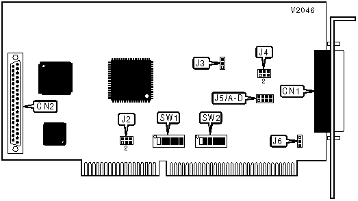
Main I/O |
CN1 |
Secondary I/O |
CN2 |
|
USER CONFIGURABLE SETTINGS | ||
|
Setting |
Label |
Position |
|
D/A converter 0 uses internal voltage reference |
J4 |
Pins 2 & 3 closed |
|
D/A converter 0 uses external voltage reference |
J4 |
Pins 1 & 2 closed |
|
D/A converter 1 uses internal voltage reference |
J4 |
Pins 5 & 6 closed |
|
D/A converter 1 uses external voltage reference |
J4 |
Pins 4 & 5 closed |
|
Timer 0 uses internal clock source |
J2 |
Pins 4 & 5 closed |
|
Timer 0 uses external clock source |
J2 |
Pins 5 & 6 closed |
|
Timers 1 and 2 use internal clock source |
J2 |
Pins 1 & 2 closed |
|
Timers 1 and 2 use external clock source |
J2 |
Pins 2 & 3 closed |
|
Pin 21 of main I/O connector outputs clock signal for counter 0 |
J3 |
Pins 2 & 3 closed |
|
Pin 21 of main I/O connector is +15VDC |
J3 |
Pins 1 & 2 closed |
|
Pin 2 of main I/O connector outputs counter 0 |
J6 |
Pins 1 & 2 closed |
|
Pin 2 of main I/O connector is -15VDC |
J6 |
Pins 2 & 3 closed |
|
BASE I/O ADDRESS | ||||||
|
Setting |
SW1/2 |
SW1/3 |
SW1/4 |
SW1/5 |
SW1/6 | |
|
0000h |
On |
On |
On |
On |
On | |
|
0010h |
On |
On |
On |
On |
On | |
|
0020h |
On |
On |
On |
On |
On | |
|
0030h |
On |
On |
On |
On |
On | |
|
0040h |
On |
On |
On |
On |
On | |
| » |
0300h |
On |
On |
On |
On |
On |
|
7FB0h |
Off |
Off |
Off |
Off |
Off | |
|
7FC0h |
Off |
Off |
Off |
Off |
Off | |
|
7FD0h |
Off |
Off |
Off |
Off |
Off | |
|
7FE0h |
Off |
Off |
Off |
Off |
Off | |
|
7FF0h |
Off |
Off |
Off |
Off |
Off | |
|
BASE I/O ADDRESS (CON’T) | |||||||
|
Setting |
SW2/1 |
SW2/2 |
SW2/3 |
SW2/4 |
SW2/5 |
SW2/6 | |
|
0000h |
On |
On |
On |
On |
On |
On | |
|
0010h |
On |
On |
On |
On |
On |
Off | |
|
0020h |
On |
On |
On |
On |
Off |
On | |
|
0030h |
On |
On |
On |
On |
Off |
Off | |
|
0040h |
On |
On |
On |
Off |
On |
On | |
| » |
0300h |
Off |
Off |
On |
On |
On |
On |
|
7FB0h |
Off |
Off |
Off |
On |
Off |
Off | |
|
7FC0h |
Off |
Off |
Off |
Off |
On |
On | |
|
7FD0h |
Off |
Off |
Off |
Off |
On |
Off | |
|
7FE0h |
Off |
Off |
Off |
Off |
Off |
On | |
|
7FF0h |
Off |
Off |
Off |
Off |
Off |
Off | |
|
Note: A total of 2048 base address settings are available. The switches are a binary representation of the decimal memory addresses. SW1/1 is the Most Significant Bit and switch SW2/6 is the Least Significant Bit. The switches have the following decimal values: SW1/2=16384, SW1/3=8192, SW1/4=4096, SW1/5=2048, SW1/6=1024, SW2/1=512, SW2/2=256, SW2/3=128, SW2/4=64, SW2/5=32, SW2/6=16. Turn off the switches and add the values of the switches that are off to obtain the correct memory address. (Off=1, On=0) | |||||||
|
D/A CONVERTER 1 OUTPUT VOLTAGE | ||
|
Setting |
J5/A |
J5/B |
|
0V to +5V |
Open |
Closed |
|
-5V to +5V |
Closed |
Closed |
|
0V to +10V |
Open |
Open |
|
-10V to +10V |
Closed |
Open |
|
D/A CONVERTER 2 OUTPUT VOLTAGE | ||
|
Setting |
J5/C |
J5/D |
|
0V to +5V |
Open |
Closed |
|
-5V to +5V |
Closed |
Closed |
|
0V to +10V |
Open |
Open |
|
-10V to +10V |
Closed |
Open |