DECISION COMPUTER INTERNATIONAL CO., LTD.
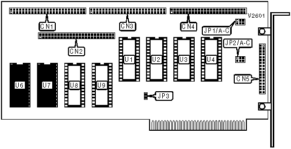
MULTI 8255/8253 CARD
|
Card Type |
Data acquisition |
|
Chip Set |
NEC 8253, 8255 |
|
I/O Options |
Digital I/O ports (4), counter port |
|
Data Bus |
8-bit ISA |

|
CONNECTIONS | |||
|
Function |
Label |
Function |
Label |
|
Digital I/O port 1 (see pinout below) |
CN1 |
8255 chip for port 4 (channel 7) |
U3 |
|
Digital I/O port 2 (see pinout below) |
CN2 |
8255 chip for port 4 (channel 8) |
U4 |
|
Digital I/O port 3 (see pinout below) |
CN3 |
8255 chip for port 1 (channel 1) |
U6 |
|
Digital I/O port 4 (see pinout below) |
CN4 |
8255 chip for port 1 (channel 2) |
U7 |
|
8253 counter port (see pinout below) |
CN5 |
8255 chip for port 2 (channel 3) |
U8 |
|
8255 chip for port 3 (channel 5) |
U1 |
8255 chip for port 2 (channel 4) |
U9 |
|
8255 chip for port 3 (channel 6) |
U2 | ||
|
CN1-CN4 PINOUT | |||
|
Function |
Pin |
Function |
Pin |
|
Channel 1A bit 0 |
1 |
Channel 1C bit 2 |
19 |
|
Channel 1A bit 1 |
2 |
Channel 1C bit 3 |
20 |
|
Channel 1A bit 2 |
3 |
Channel 1C bit 4 |
21 |
|
Channel 1A bit 3 |
4 |
Channel 1C bit 5 |
22 |
|
Channel 1A bit 4 |
5 |
Channel 1C bit 6 |
23 |
|
Channel 1A bit 5 |
6 |
Channel 1C bit 7 |
24 |
|
Channel 1A bit 6 |
7 |
Ground |
25 |
|
Channel 1A bit 7 |
8 |
Ground |
26 |
|
Channel 1B bit 0 |
9 |
Channel 2A bit 0 |
27 |
|
Channel 1B bit 1 |
10 |
Channel 2A bit 1 |
28 |
|
Channel 1B bit 2 |
11 |
Channel 2A bit 2 |
29 |
|
Channel 1B bit 3 |
12 |
Channel 2A bit 3 |
30 |
|
Channel 1B bit 4 |
13 |
Channel 2A bit 4 |
31 |
|
Channel 1B bit 5 |
14 |
Channel 2A bit 5 |
32 |
|
Channel 1B bit 6 |
15 |
Channel 2A bit 6 |
33 |
|
Channel 1B bit 7 |
16 |
Channel 2A bit 7 |
34 |
|
Channel 1C bit 0 |
17 |
Channel 2B bit 0 |
35 |
|
Channel 1C bit 1 |
18 |
Channel 2B bit 1 |
36 |
|
CN1-CN4 PINOUT (CON’T) | |||
|
Function |
Pin |
Function |
Pin |
|
Channel 2B bit 2 |
37 |
Channel 2C bit 1 |
44 |
|
Channel 2B bit 3 |
38 |
Channel 2C bit 2 |
45 |
|
Channel 2B bit 4 |
39 |
Channel 2C bit 3 |
46 |
|
Channel 2B bit 5 |
40 |
Channel 2C bit 4 |
47 |
|
Channel 2B bit 6 |
41 |
Channel 2C bit 5 |
48 |
|
Channel 2B bit 7 |
42 |
Channel 2C bit 6 |
49 |
|
Channel 2C bit 0 |
43 |
Channel 2C bit 7 |
50 |
|
Note:CN2 through CN4 are wired identically to CN1. CN1 has the signals for channels 1 and 2. CN2 through CN4 have the signals for channels 3 through 8, respectively. | |||
|
CN5 PINOUT | |||
|
Function |
Pin |
Function |
Pin |
|
Ground |
1 |
Counter 2B clock signal in |
18 |
|
Counter 1A clock signal in |
2 |
Gate 2B signal |
19 |
|
Gate 1A signal |
3 |
Counter 2B clock signal out |
20 |
|
Counter 1A clock signal out |
4 |
Ground |
21 |
|
Ground |
5 |
Counter 2C clock signal in |
22 |
|
Counter 1B clock signal in |
6 |
Gate 2C signal |
23 |
|
Gate 1B signal |
7 |
Counter 2C clock signal out |
24 |
|
Counter 1B clock signal out |
8 |
Ground |
25 |
|
Ground |
9 |
+5V DC power |
26 |
|
Counter 1C clock signal in |
10 |
Ground |
27 |
|
Gate 1C signal |
11 |
-5V DC power |
28 |
|
Counter 1C clock signal out |
12 |
Ground |
29 |
|
Ground |
13 |
+12V DC power |
30 |
|
Counter 2A clock signal in |
14 |
Ground |
31 |
|
Gate 2A signal |
15 |
-12V DC power |
32 |
|
Counter 2A clock signal out |
16 |
Ground |
33 |
|
Ground |
17 |
Ground |
34 |
|
USER CONFIGURABLE SETTINGS | |||
|
Setting |
Label |
Position | |
| » |
Counter 1A uses internal clock source |
JP1/A |
Closed |
|
Counter 1A uses external clock source |
JP1/A |
Open | |
| » |
Counter 1B uses internal clock source |
JP1/B |
Closed |
|
Counter 1B uses external clock source |
JP1/B |
Open | |
| » |
Counter 1C uses internal clock source |
JP1/C |
Closed |
|
Counter 1C uses external clock source |
JP1/C |
Open | |
| » |
Counter 2A uses internal clock source |
JP2/A |
Closed |
|
Counter 2A uses external clock source |
JP2/A |
Open | |
| » |
Counter 2B uses internal clock source |
JP2/B |
Closed |
|
Counter 2B uses external clock source |
JP2/B |
Open | |
| » |
Counter 2C uses internal clock source |
JP2/C |
Closed |
|
Counter 2C uses external clock source |
JP2/C |
Open | |
| » |
Base I/O address set to 140h |
JP3 |
Closed |
|
Base I/O address set to 100h |
JP3 |
Open | |